

Product comparison
Wafer Diameter
Accuracy
Resolution
Spartial Resolution
Scans
Dynamic Range
Software
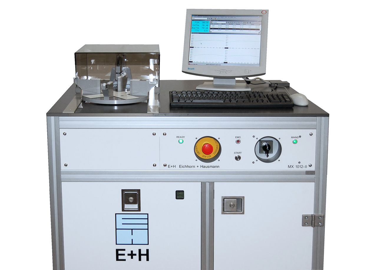
4“, 5“, 6“
±0.1 µm
10nm
1mm
4
100 or 350µm
MXNT
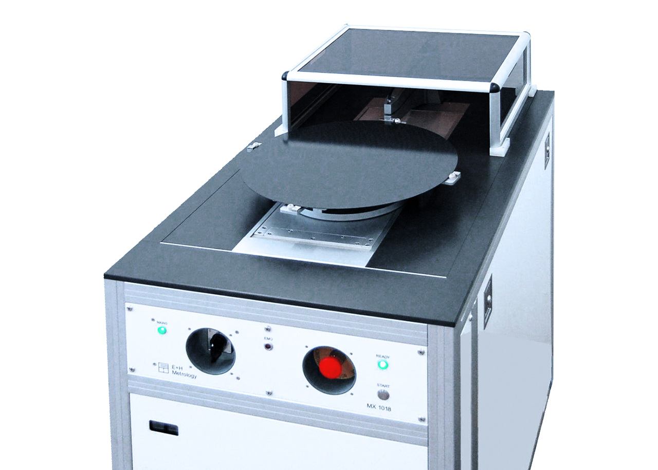
6“, 8“
±0.1 µm
10nm
1mm
4
100 or 350µm
MXNT
8", 12"
±0.1 µm
10nm
1mm
up to 8
100 or 350µm
MXNT
12", 18"
±0.3 µm
10nm
1mm
up to 8
100 or 350µm
MXNT
Scroll down for more
Related products

Scroll down for more
WHICH TOOL
fits my needs?
You have questions, wishes or an order?
We will be happy to consult you personally.

Scroll down for more