Related products
Scroll down for more
WHICH TOOL
fits my needs?
You have questions, wishes or an order?
We will be happy to consult you personally.

Scroll down for more

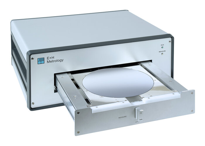
Fast contactless geometry gauge for 2–4" non-conductive and semi-insulating wafers.
High throughput: the MX203-4-37-Q gauges with its 37 measuring points every wafer within max. 10 seconds. It controls thickness and flatness. Flexible wafer size adjustment by various centering-frames. Suitable for wafers made of non-conductive substrates (Quartz, Saphire, Lithium Niobate, Lithium Tantalate) and semi-insulating materials like Gallium Arsenide or Silicon Carbide. Comes with our powerful MX-NT operating software.
| Wafer Diameter | 50mm, 75mm, 100mm |
| Accuracy | ±1 µm |
| Resolution | 0.1µm |
| Thickness range | 300 - 800 µm |
| Non-conductive substrates | yes |
| Semi-insluation materials | above 107 Ohm*cm |
| Software | MXNT |
You have questions, wishes or an order?
We will be happy to consult you personally.