
Contract measurement
and measurement strategies
You only need to measure wafers occasionally, have small quantities or the acquisition of your own measuring equipment is not (yet) economically viable? Your business is still at the very beginning and needs sporadic measurement solutions? You are reorganizing your production and would like a consultation for your measurement strategy? Use the knowledge from more than 50 years of expertise in the field of semiconductor measurement. Secure relevant competitive advantages in a resource-efficient way!
- Contract measurements for semiconductor wafers in all sizes
- Various materials
- Consulting for your measurement strategy
- Expert know-how at the best price
Your advantages
at a glance
We make your successes measurable: We are happy to make our know-how from the last 50 years available to you for your processes. The advantages for you:
- Professional measurements by experts: Our team is made up of long-standing specialists in the semiconductor industry.
- Application of state-of-the-art measurement technology: Our systems cover all relevant surface and geometry measurement methods.
- Coordinating the best individual measurement strategy: Which characteristics do you need to measure in which process step? In which time intervals is this particularly helpful for you? Which measurement method is the most resource-saving for you? We clarify all this with you in a measurement strategy consultation.
- Data visualization in 3D: Using the impressive features of our 3D visualization via WaferStudio, you and your team will not only become more efficient, but also capable of making interdisciplinary decisions, for example regarding process optimization for your fabrication.
- Evaluation of your measurement data for you: The measurement data is transmitted to you in a Microsoft Excel-compatible CSV format (Comma Separated Value).
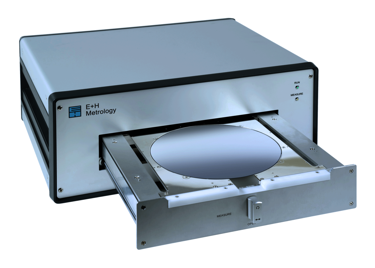
OUR services
We inspect a wide variety of materials & probes for you:
- Semiconductor wafers
- Photovoltaic wafers
- Sizes from 50mm (2“) to 450 mm (18“)
- Round and (pseudo)square forms
- Special forms (Taiko, framed), Silikon blocks, wafer pieces
- Special materials: non-conductive substrates (Quartz, Saphire, Lithium Niobate, Lithium Tantalate) and semi-insulating materials like Gallium Arsenide or Silicon Carbid
Depending on your requirements we characterize:
“We were able to significantly improve our machines thanks to the precise contract measurement provided by E+H.”
Customer Contract Measurement, 2022
CONTRACT MEASUREMENT
required?
Do you have questions about our services, times and costs? Simply fill out the form and we will get back to you promptly.

Sebastian Königsmann