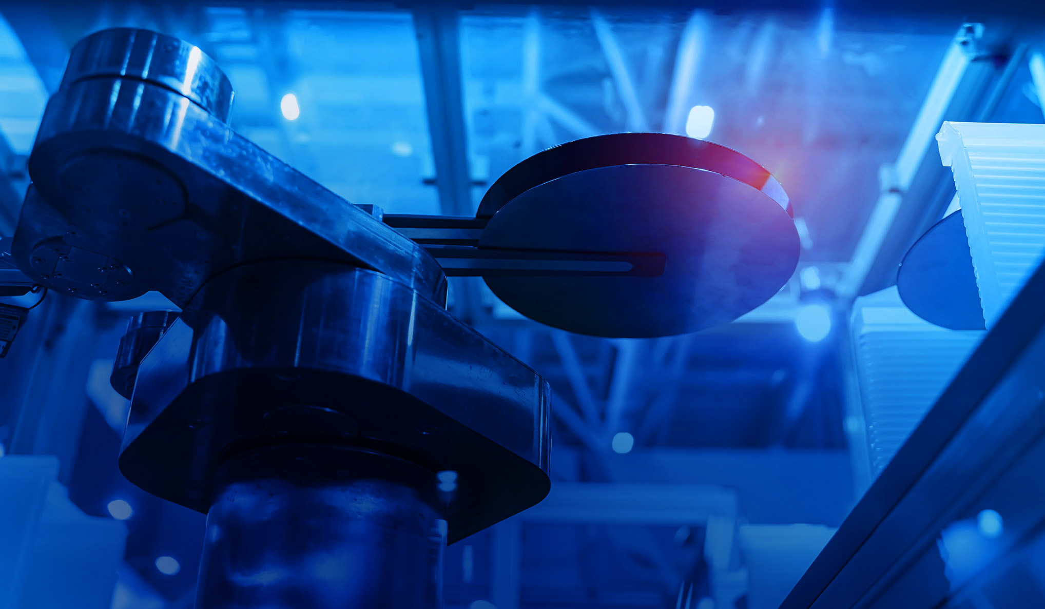

WAFER RECLAIM
EFFICIENCY STARTS
with the material
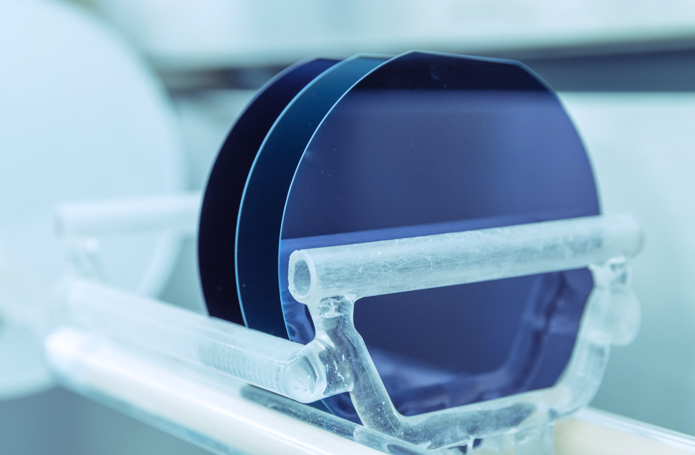
Supply bottlenecks, diversified requirements and exploding costs at the same time: High-quality material such as silicon or gallium arsenide is the linchpin of the semiconductor industry - and at the same time its Achilles’ heel. With ever larger substrate diameters, material is becoming a growing challenge. No wonder many wafer fabs today employ a consistent reclaim strategy for their test wafers in particular. Efficient reclaiming and recycling requires measurable reliability:
- Sorting, stripping, lapping and grinding, polishing & cleaning: measure all reclaiming steps in a process reliable way.
- Cost-effective and reproducible measurement systems for reclaim & recycling
- Sophisticated, individual automation solutions
- Special materials: glass, quartz, gallium arsenide, etc.
- Fast tools with high throughput up to 1,000 wafers per hour
WAFER RECLAIM:
(R)evolution of Efficiency
The global pandemic has painfully crystallized a fundamental problem of the semiconductor industry:
Barely manageable material costs and disruption-prone supply chains determine market dynamics.
The very costly wafer and chip production in particular benefits from recycling and reclaiming the expensive semiconductor materials.
At E+H, we see ourselves not only as experts for high technology. Our task is to work with you to make your processes more efficient:
- Size matters: we offer highly efficient, slim measurement systems for all wafer sizes from >50 to 450 mm.
- Material matters: our measuring devices are ideally suited for all high-resistance materials.
- Process efficiency matters: Boosting throughput while keeping maintenance to a minimum: Our specialists develop the most efficient test and measurement process in close cooperation with you. Consulting our customers at eye level for more than 54 years makes us as proud as we are competent: Count on our commitment to your Reclaim processes.
APPLICATIONS


“Consulting is very essential. With E+H, we always find a solution - even for very specific requirements.”
Customer · From: E+H customer & partner survey 2021

HOW CAN WE HELP?
Contact our team.
Do you have further questions? We will be happy to advise you personally.
Peter Michel
+49 (0)721 83118-17