NANOTOPOGRAPHY MEASUREMENT
in Semiconductor industry
Nanotechnology is considered one of the key technologies of the 21st century. The increasing miniaturisation is first and foremost affecting the semiconductor industry. Ever finer structure sizes enable ever better chip performance.
The performance requirements for modern semiconductor components are constantly increasing. As a result, ever better high-performance measurement technology for the nano and subnanometre range is indispensable. Including technology that is as innovative as it gets.
What is semiconductor measurement missing at the nanoscale?
State-of-the-art measurement methods follow different approaches. However, most of them have significant weaknesses:
- A large measuring field with simultaneously high resolution is thus not achieved: Both 3D microscopes (high resolution but small measuring field) and macroscopic 3D sensors (large measuring field but only macroscopic resolution) for themselves do not solve the problem.
- Present measuring devices are susceptible to vibrations: Until now, unevenness in the nanometre range has been detected using optical interferometry. But even the most modern tools are very sensitive to the slightest vibrations - which makes cost-effective integration in wafer fabs almost impossible.
- Until now, only qualitative measurement results have been possible: the conventional Makyo systems reach their natural limits here. They do provide 2D greyscale images that make irregularities on a surface visible. However, they do not provide any information about the actual height.
A new approach: Full surface inspection in nanometer range
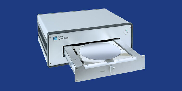
Our research and development team has dedicated itself to these problems - with revolutionary results that we have integrated into our „Global Nanoscope“ metrology system.
-
Measuring the entire surface at once without stitching: Our newly developed method bridges the gap between all previously used measurement methods in the field of nanometric measurement of specular surfaces. At present, we can measure nanostructures on wafers with a diameter of up to 300 mm within 60 seconds.
-
Reliable measurement - regardless of vibrations: The fully motionless and contactless, non-destructive surface inspection is another advantage. The system has proven to be fully robust against external influences such as vibrations. There are no moving parts during the inspection.
-
Qualitative and quantitative measurement results at once: Standard Makyoh images provide two-dimensional, blurred images. The system based on E+H Advanced Makyoh gains real height information of the surface. It enables us to perform both a qualitative and a quantitative measurement.
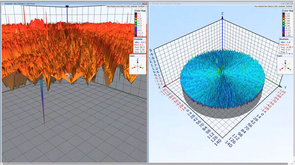
Taken from our 3D software Waferstudio: Nanometric surface measurement based on our Advanced Makyoh process.
RECOMMENDED PRODUCTS
WHICH CHARACTERISTICS
do you need to measure?
You have questions, wishes or an order?
We will be happy to consult you personally.
