
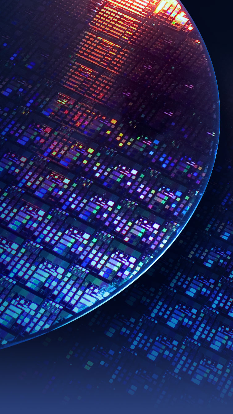
SEMICONDUCTOR & MEMS
The measure
of success
Semiconductor and MEMs metrology is always pushing the envelope. We take it one step further and realize for you what you really need, exactly as you need it: whether for classic semiconductor wafer measurements or mems inspection:
- Fast, high-precision wafer geometry measurement in the subnano range
- Mature Measurement gauges for a wide range of high resistivity materials
- Individual engineering, automation and integration for your process requirements
- Customized capacitive and deflectrometric measurement methods
- Unique 3D visualization with Waferstudio software
- Reproducible measurements for all relevant wafer characteristics

RAISE PROFILE
Wafer Metrology
You want more than what is possible. You want a solution. Traceable, market-leading fast and innovative semiconductor metrology tools from the experts in high technology:
- Contactless, individual sensor measurement for wafers up to 450 mm in diameter.
- Exact, reproducible results without unnecessary and cost-intensive data deluge
- Easy to operate
- Low maintenance and long lifetime
Made to measure
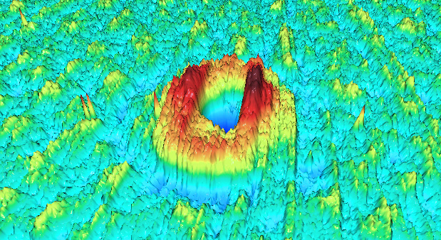
VISUALIZE
Intuitive 3D analysis software
You need process reliability at a glance? That’s why we developed Wafer Studio: our powerful 3D analysis software is the only manufacturer independent tool on the market. It offers you exact visualizations of your measurement results within seconds. Wafer Studio allows process optimization, efficient evaluation and solid documentation.
- Easy creation of 3D visualization of wafer maps
- wafer maps 7 different interpolation methods
- Before/after visualization
- For wafers, chips, reclaim and solar
OPTIMIZE PROCESSES
Increase throughput
Faster and faster, more and more: Production processes and automation in semiconductor, MEMs and chip manufacturing need stability and repeatability to meet these requirements.
Today being competitive requires extremely fast, smooth and flexible processes. Processes must also be controllable, plannable and manageable down to the smallest detail. As your partner for measurement technology and process optimization, we make complex things simple. Our expertise from more than 50 years and our custom-developed systems are geared to providing the best solution for your needs: increasing your throughput with optimized processes, efficient automation and technology made to measure.
APPLICATIONS


“The products are extremely reliable, stable, cost-effective and easy to use - with very high performance.”
Customer · From: E+H customer & partner survey 2021

HOW CAN WE HELP?
Contact our team.
Do you have further questions? We will be happy to advise you personally.
Peter Michel
+49 (0)721 83118-17