WAFER GEOMETRY MEASUREMENT
with highest throughput

THICKNESS
A consistent thickness is crucial for the manufacturing process of silicone wafers. Every further manufacturing step is based on this.
Our gauges measure the wafer thickness quickly, highly precisely and always reproducibly. The wafer is gauged contactless and unmoved via capacitive sensors.
Thin-wafer technology has been conquering modern industries for more than a decade: from household appliances to hybrid drives, chips made from wafers between 200 and 40 micrometres thick provide energy savings of up to 40%. As demand increases, so does the demand for productivity: reliable and, above all, fast measurements support this more than anything else.
Our measuring tools for wafer thickness enable a short measuring time that is unique in the market for all wafer types from thin wafers to conventional thicknesses..

TOTAL THICKNESS VARIATION
The thickness variation describes the maximum difference between the thinnest and thickest point of the measured wafer.
This key indicator (TTV value) is highly relevant to quality in wafer production: Only wafers with a low TTV value can be used for sophisticated tasks.
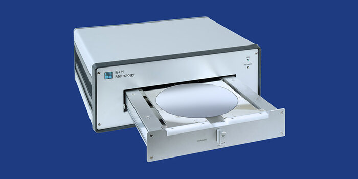
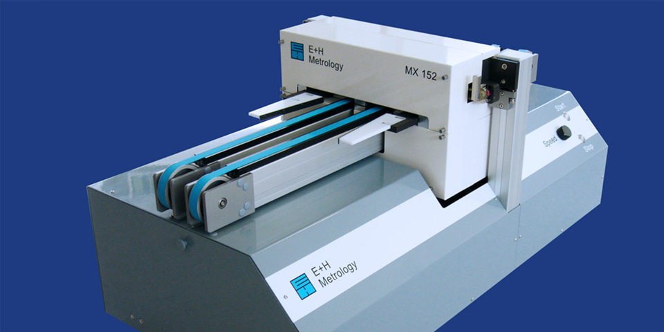
We offer TTV measuring systems for all applications: particularly cost-efficient manual devices for material thicknesses from 100 µm up to fully automated applications for wafers up to 970 µm thick. Our proven multi-sensor technology achieves resolutions down to the nanometer range.
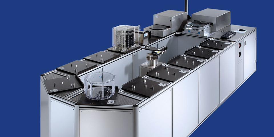
In wafer manufacturing, many different steps follow one another. And all of them require reliable monitoring of the TTV value and others. Already during wire sawing and edge grinding/rounding, cleaning, grinding and lapping or etching, this key figure determines the entire production workflow.
We offer you the right metrology system for every process step in your production chain with unique throughput and maximum cost efficiency.

WARP, BOW & SORI
The flatness of any material is decisive for the success or failure of Wafer manufacturing.
Bow is the deviation of the centre of the surface of a wafer from the reference plane. Warp is the sum of the maximum positive and negative deviations from the reference plane.
Our measuring instruments cover all basic measurement parameters of wafer flatness or wafer geometry at once: TTV, Bow, Warp and also Sori.
Bow and warp must be continuously monitored, especially in the final production steps in the wafer fab: Wafer packaging requires efficient processes and reproducible measured values.
Our measuring systems make this possible - with uniquely low maintenance and an exceptionally high durability.

FILM STRESS
During chip manufacturing processes, up to several hundred layers are applied to the wafer. In order to achieve the maximum yield, reliable control of the film stress is crucial for a continuous production process.
Film stresses cannot be measured directly. The radius of curvature can only be determined by measuring the bowing of the substrate. In addition to an exact wafer geometry measurement, some of our systems simultaneously offer an evaluation of the film stress of the examined substrate for this purpose.
What makes our measurement method so unique?
- We measure when the wafer is at rest: disruptive movements can massively impair reproducibility.
- The wafer lies stably on three contact points.
- We work without vacuum technology, which can also falsify your measurement results and reference values.
With our automatic system MX2012-H, the throughput of the system is 100 wafers per hour or more. All our systems are extremely lowmaintenance, ensuring you an exceptionally cost-effective, efficient testing process.
Background: Unfavorable component film stress can have a relevant impact on the lifetime of the product manufactured from the material. The shortening of the lifetime is a major problem that causes millions of dollars in service and warranty costs annually.
RECOMMENDED PRODUCTS
WHICH CHARACTERISTICS
do you need to measure?
You have questions, wishes or an order?
We will be happy to consult you personally.
