Related products
Scroll down for more
WHICH TOOL
fits my needs?
You have questions, wishes or an order?
We will be happy to consult you personally.

Scroll down for more

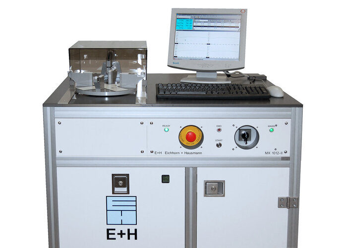
Combined thickness and resistivity gauge for 200 mm and 300 mm silicon wafers.
The MX6012 is designed to characterize silicon wafers. It combines contactless thickness, resistivity and P/N dotation sensors. In addition to the center measurement, up to 15 additional points for each half scan can defined. Optionally an identical scan after 90° rotation. To be connected to a PC via serial interface. Comes with our powerful MX-NT operating software. Integration into automatic robotic sorter systems possible.
| Wafer Diameter | 200, 300 mm |
| Thickness | 600 – 900 μm |
| Max. Warp | 100 μm |
| Resistivity | 0.001 – 200 Ohm·cm |
| Type check | 0.020 – 200 Ohm·cm |
| Software | MXNT |
You have questions, wishes or an order?
We will be happy to consult you personally.